PSL wafer standards are crucial in the semiconductor manufacturing field, as they enable precise measurement and control of particle size and morphology on wafer surfaces. This is decisive for ensuring the quality and reliability of semiconductor devices. Throughout the entire production process from wafer fabrication to packaging and testing, PSL wafer standards consistently play a key role in ensuring semiconductor devices fully comply with the industry’s stringent quality and reliability standards.
Definition of PSL Wafer Standards
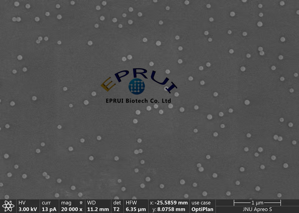
Polystyrene (PSL) particle size standards are used, depositing spherical PSL particles onto the surface of a prime silicon wafer or onto a substrate like a quartz photomask. Wafer standards are produced as full-deposition, spot-deposition, and half-deposition wafers. Full-deposition wafers have a single particle diameter deposited across the entire wafer surface. Half-deposition wafers have particles deposited on only one side of the wafer. Spot-deposition wafers deposit 1 to 10 particle sizes as spots on the surface of a 300mm wafer standard, typically located at the wafer edge, but they can be deposited anywhere on the wafer surface per customer requirements. Full-deposition wafer standards provide one particle size, serving as a single size calibration point for the wafer inspection system being calibrated. Experienced metrology engineers also observe the uniformity of the wafer inspection system in detecting particles of the same size while scanning the entire wafer surface. Half-deposition wafer standards provide one particle size as a size calibration point for the wafer inspection system. This also allows metrology engineers to see the difference in the wafer inspection system’s laser response between the particle-coated side and the clean side of the standard. Spot-deposition wafer standards are typically the most demanded by today’s more advanced wafer inspection systems (such as KLA-Tencor SP1, SP2, SPx). For example, a 300mm spot-deposition wafer standard might have 8 size peaks deposited around the wafer, ranging potentially from 30nm to 2 microns. When an SSIS tool or wafer inspection system scans these 8 sizes during a single scan of the wafer standard, it can assess the calibration of the wafer inspection system across its entire dynamic size response range.
The Role of PSL Wafer Standards in Semiconductor Manufacturing
1. Calibration and Verification of Particle Measurement Instruments
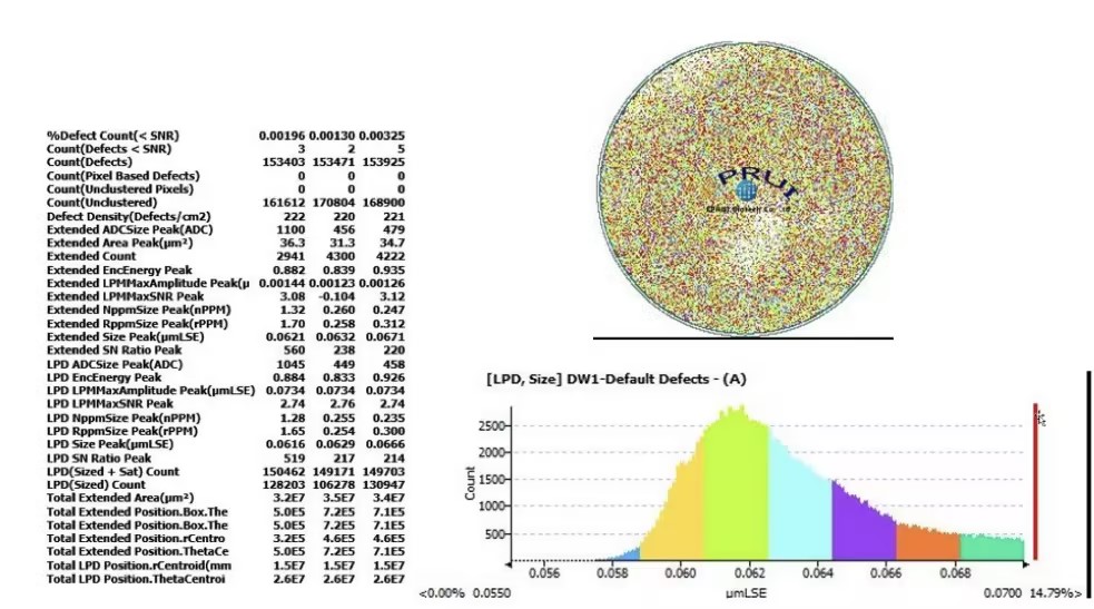
PSL wafer standards are core tools for instrument calibration and performance verification. Specific-sized PSL microspheres (e.g., 0.1µm, 0.2µm, 0.5µm) are deposited onto the wafer through precise processes. These microspheres have uniform size, perfect sphericity, and stable optical properties. During calibration, measurement instruments detect these PSL particles with known size and distribution. By comparing the measurement results with the standard values, the instrument’s size response curve (calibration curve) can be precisely established or corrected, ensuring accurate size reporting across the instrument’s entire measurement range.
Furthermore, it serves as an objective benchmark for evaluating the comprehensive performance and compliance of instruments. Beyond size calibration, PSL standards are used to verify key instrument performance metrics such as detection efficiency (ability to capture particles), counting accuracy, resolution, and repeatability. Under the framework of strict industry standards like ISO 14644 and SEMI, regularly using PSL standards to verify measurement instruments is a mandatory procedure to demonstrate their continued compliance with process monitoring requirements and to ensure data reliability. This directly relates to the accurate assessment of cleanroom class and particle emission rates from process tools.
These standards are used to calibrate and verify particle measurement instruments, such as Scanning Electron Microscopes (SEM) and Optical Particle Counters (OPC), which are used to monitor and control particle contamination during semiconductor manufacturing.
By adopting PSL wafer standards, semiconductor manufacturers can ensure the accuracy and reliability of their particle measurement instruments, which is essential for maintaining high yield and high quality in semiconductor manufacturing.
2. Monitoring and Control of Particulate Contamination
In addition to calibrating particle measurement instruments, PSL wafer standards are also used to monitor and control particle contamination in semiconductor manufacturing processes. By adopting PSL wafer standards, semiconductor manufacturers can ensure their manufacturing processes are free from particle contamination, which is crucial for preventing defects and yield loss in semiconductor devices.
Pollution control in modern cleanrooms is a dynamic systems engineering task, encompassing the process equipment itself, local purification units (SMIF/FOUP), and the entire facility system. PSL standards are not only used for instrument calibration but are also actively employed as challenge test particles. For example, by controllably introducing them into a specific environment or equipment chamber and then using monitoring instruments for tracking measurements, one can quantitatively assess and verify: How efficient is the local purification? Does the equipment meet its claimed particle emission rate? Is the wafer transfer process truly contamination-free? This “stress test” based on standard particles transforms abstract pollution control capabilities into concrete, quantifiable performance indicators, serving as the scientific basis for implementing preventive maintenance and continuous improvement.
When yield loss occurs on the production line due to particles, traceability analysis relies heavily on deep mining of historical monitoring data. Reliable historical data, strictly calibrated using PSL standards, enables engineers to accurately determine the start time, size distribution characteristics, and possible source range of a contamination event. Without a unified and accurate standard, data noise would obscure the true signal, delaying problem resolution. Furthermore, when introducing new processes or equipment, using PSL standards for baseline performance confirmation is a standard operation for preventing contamination risks and establishing initial control limits.
PSL wafer standards transcend the role of a mere calibration tool. By providing an indisputable metrological benchmark for the entire particle monitoring network, they transform scattered measurement data into credible “contamination intelligence,” thereby supporting a complete chain from precise monitoring and system verification to root cause analysis and preventive control. They are the “keystone” at the microscopic scale that safeguards the ultra-clean environment of semiconductor manufacturing and achieves the goal of nanometer-level process yield.
3. Verification of Cleaning Processes and Equipment
PSL wafer standards can also be used to verify cleaning processes and equipment (such as wet benches and cleanrooms), which are crucial for maintaining a clean production environment within semiconductor manufacturing facilities.
Evaluating the cleaning efficiency of wafer cleaning tools, dry cleaning processes, or chemical formulations cannot be accurately quantified merely by visual or electrical testing of the final wafer. Operators simulate a “deliberately contaminated wafer” by processing a standard wafer deposited with specific-sized and known-quantity PSL microspheres through the cleaning process to be verified. After processing, a surface particle detector is used to precisely count and analyze the size of residual particles. By comparing the particle counts before and after processing, the removal rate of the cleaning process for different particle sizes can be precisely calculated. This provides direct, quantitative data for process optimization, formulation comparison, and setting qualification standards.
As a “standardized test particle” for equipment and subsystem cleanliness, when equipment (such as etchers, thin-film deposition equipment) is installed, maintained, or periodically monitored, it is necessary to verify the “particle emission” level of its chambers and transfer systems. Using a PSL standard as a “clean monitor wafer” placed into the equipment, running a simulated process cycle, and then detecting newly added particles on its surface achieves this. To precisely distinguish and quantify particles generated by the equipment itself, PSL microsphere aerosols are sometimes actively introduced into specific areas of the equipment, and their removal effectiveness or diffusion is monitored. This method can quantitatively assess the design effectiveness of the equipment’s internal purging airflow, the particle generation from wear of mechanical moving parts, and the recovery status after maintenance.
PSL standards transform the abstract concept of “cleanliness” into measurable, reportable, and comparable engineering parameters. By providing stable and reliable “simulated contaminants,” they enable the precise calibration and continuous monitoring of the cleanliness performance of cleaning processes and equipment themselves. They are a foundational tool for building a high-technology, high-reliability cleanliness system in semiconductor manufacturing.
Conclusion
PSL wafer standards permeate every aspect of semiconductor manufacturing, from monitoring and verification to analysis. By establishing a precise “measurement standard” for the microscopic world, they transform cleanliness control from experience-based to data-driven. They are indispensable underlying infrastructure supporting modern semiconductor manufacturing’s advancement towards higher precision, higher yield, and higher reliability.
EPRUI Biotech Co., Ltd. has been dedicated to the field of monodisperse microsphere materials for over decades. Its monodisperse microspheres—including polystyrene microspheres, PMMA microspheres, silica microspheres, fluorescent microspheres, streptavidin microspheres, and magnetic microspheres—are widely utilized in various critical applications. These versatile materials are widely used in various industries such as biomedicine, liquid crystal display (LCD), analytical testing, in vitro diagnostics, and instrument calibration.
The copyright belongs to EPRUI Biotech Co., Ltd. All rights reserved! Welcome to repost with a link to the original source. Illegal reproduction will be pursued for legal responsibility!