On a chip as small as a fingernail, billions of transistors are integrated. The manufacturing process is akin to “building a skyscraper on the tip of a needle.” The wafer, as the foundation of the chip, can be rendered useless by any tiny defect. Wafer defect inspection is the “quality inspector” of chip manufacturing. Using sophisticated techniques to detect micron- and even nanometer-scale flaws is a core process for ensuring chip yield. To ensure inspection accuracy, those calibration spheres such as PSL calibration particle, silica standard microspheres play a very important role.Lorem ipsum dolor sit amet, consectetur adipiscing elit.Ut elit tellus, luctus nec ullamcorper mattis, pulvinar dapibus leo.
I. Invisible “Fatal Flaws”: What Are the Types of Wafer Defects?
Wafer defects can be classified by morphology into surface defects, internal defects, and lattice defects. Though tiny, their impact is fatal.
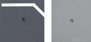
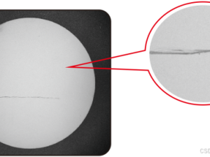
Scratches/Cracks: Caused by mechanical friction or thermal stress during production, they damage circuit structures and can even cause the wafer to fracture.
Residues/Contamination: Chemical residues left after etching or cleaning, which interfere with semiconductor conductivity and cause current leakage.
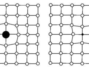
Lattice Defects: Disordered arrangement of silicon atoms (e.g., vacancies, dislocations). These “internal injuries” reduce chip stability and shorten service life.
- How to Detect Micro-Defects? Overview of Mainstream Inspection Technologies
Chip manufacturing has entered the 3nm/2nm era, with defects as small as a few nanometers,which is completely invisible to the naked eye. Therefore, high-precision equipment is essential, and there are three core inspection technologies.
- Optical Inspection: The Fastest “Census Taker”
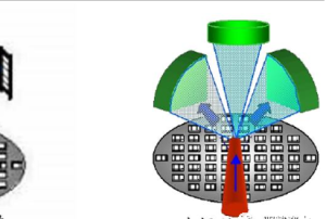
Based on light scattering, this is the mainstream industrial technology, with bright-field and dark-field modes.
- Dark-field detection (mainstream): Laser illuminates the wafer at an oblique angle. Light reflects away from defect‑free areas, while defects (particles, scratches) scatter light. High-sensitivity sensors capture the scattered light, accurately locating nanoscale defects. It can detect 0.1μm particles at speeds up to 200 wafers per hour.
- Bright-field detection: Vertical illumination captures reflected light, suitable for larger defects such as photoresist residues or pattern shifts.
- Electron Beam Inspection: Nanoscale “Magnifying Glass”
Uses a scanning electron microscope (SEM) to emit high-energy electrons to scan the wafer, imaging via electron signals. Resolution reaches 1nm, allowing atomic-scale defects to be seen. Suitable for precision inspection of advanced nodes (e.g., 3nm FinFET), but slower, mostly used for spot check.
- Calibration Technology: The “Fixed Star” of Inspection Accuracy
No matter how precise the equipment, it needs a “ruler” for calibration. Particles with precisely controlled particle size for simulating defects in wafer defect inspection equipment such as PSL calibration spheres, silica calibration particles are the “standard weights” of the semiconductor industry.
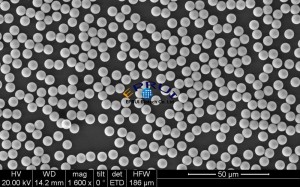
- PSL calibration spheres (polystyrene latex microspheres): Precisely controlled particle size:50nm–100μm, perfect spherical shape,narrow particle size distribution(CV ≤3.5%) which help simulate surface particles to calibrate traditional low-power inspection tools (e.g., KLA-Tencor SP1/SP2).
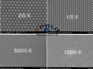
- Silicacalibrationmicrospheres: Precisely controlled particle size: 20nm–100μm, perfect spherical morphology,narrow particle size distribution (CV ≤3.5%), high temperature resistance (>1600°C), resistant to DUV/EUV lasers,which is suitable for next-generation high-power inspection tools (e.g., KLA-Tencor SP3/SP5). Its service life is 3–5 times longer than PSL particles.
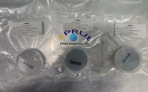
- Wafer calibration standards: Precision particles (PSL or silica) deposited on silicon/glass wafers, uniformly distributed across the entire wafer. Used for daily equipment calibration, sensitivity verification, and ensuring consistent data across different production lines.
III. Why is Defect Inspection So Important? Yield is the Lifeline
Chip manufacturing involves over 500 process steps, each step can introduce defects. Defect inspection directly determines chip yield and production cost. Therefore, it is always a core concern for global semiconductor manufacturers.
- A single 100nm particle can scrap an entire 12inch wafer (worth tens of thousands of dollars). If defect inspection can help reduce chip yield loss by 1%,then over ten million dollars costcan be saved for a production line annually.
- Defect data drives process optimization: By identifying the source of defects (e.g., etcher parameter drift, cleaning fluid contamination), manufacturers can continuously improve processes, raising yield from 90% to 99% and effectively doubling capacity.
- Essential for advanced nodes: As process nodes move toward 3nm, 2nm and beyond, defect inspection precision requirementsalsoincrease. High accuracy inspection and calibration technologies are prerequisites for volume production of advanced chips, and are key to ensuring chip performance and reliability.
- Future Trends: Smaller, Faster, Smarter
As chip manufacturing advances toward 2nm and 1nm, wafer defect inspection faces the triple challenge of smaller scales, higher speeds, and greater precision – while also presenting new opportunities for innovation.
- Technology upgrades: Extreme ultraviolet (EUV) inspection technology is becoming more widespread, enabling precise detection of 1nm defects. Deep learning AI can automatically classify defects with >99% accuracy, greatly improving inspection efficiency.
- Calibrationparticles innovation: Silica nanospheres are gradually replacing traditional PSL nanospheres to better match highenergy EUV inspection tools. Customized calibration wafers (with tailored particle sizes and densities) can meet the inspection needs of different advanced nodes.
- Closedloop process: From wafer manufacturing and defect inspection to process optimization and re-inspection, a complete data loop helps global semiconductor manufacturers pursue a “zero-defect” production goal.
Conclusion
Wafer defect inspection is the guardian of chip manufacturing. The seemingly unremarkable PSL calibration particles, silica calibration spheres as well as calibration wafers are actually the core foundation supporting the precision of the entire semiconductor industry. In the ongoing wave of global semiconductor technology iteration, overcoming bottlenecks in defect inspection and calibration technology is not only a matter of business competition but also a necessity for the sustainable development of the global chip industry. As technology continues to evolve, human beings will be able to detect even smaller wafer defects, making chips around the world more reliable and more powerful.