Project Description
Calibration Wafer Standards Use PSL Particles
In the semiconductor industry, the SSIS Scanning Surface Inspection System is a critical piece of equipment primarily used to detect defects on wafer surfaces, such as particles, scratches, residues, crystal defects, and so on. The SSIS system is vital to the semiconductor manufacturing process because even microscopic surface defects can significantly impact chip performance and yield.
EPRUI Biotech Co., Ltd. can provide PSL size standard spheres with particle sizes ranging from 20 nm to 100 μm. Dimensional accuracy is ensured through measurement methods such as TEM, SEM, and laser particle size analysis. Through actual testing, the particle size accuracy of our product is comparable to the quality of Surf-Cal standard particles.
EPRUI Biotech Trusted By


Complete Buying Guide of PSL Calibration Particles for Wafer/Photomask Defect Inspection Equipment
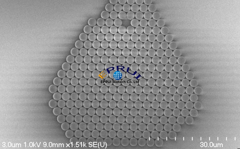
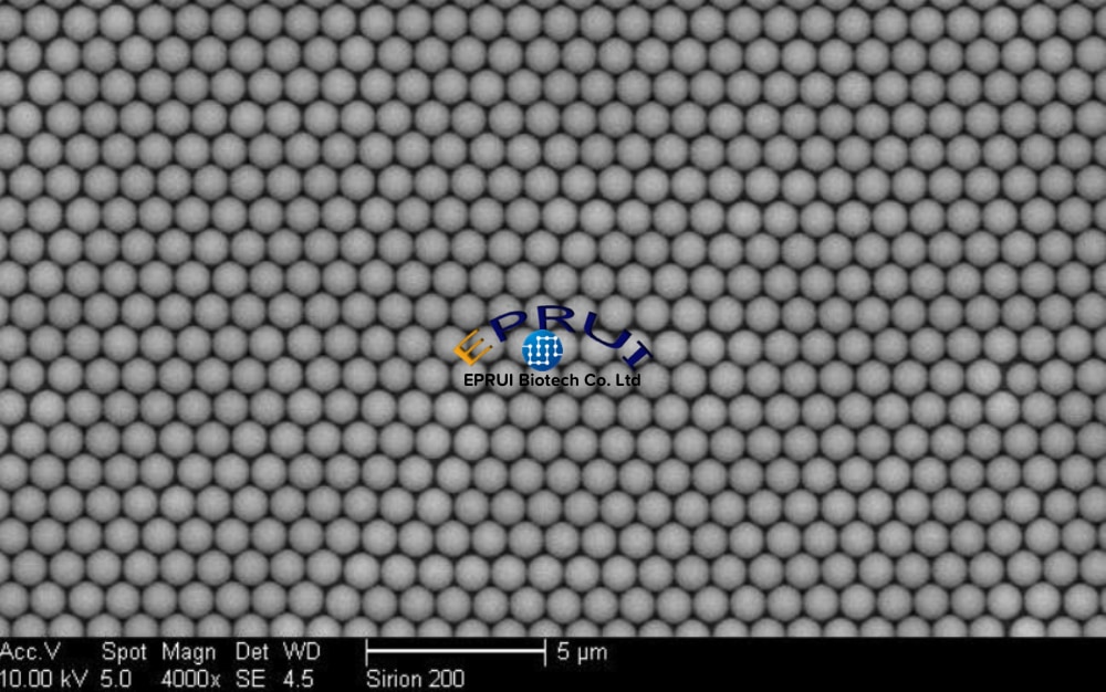
Monodisperse PSL/Polystyrene latex microspheres are key metrology tools in the semiconductor industry.Due to its highly uniform particle size with narrow particle size distribution, perfectly spherical geometry,predictable light-scattering behavior and strong contrast in both bright-field and dark-field illumination,PSL (Polystyrene Latex) microspheres are still the industry standard for optical inspection calibration.
1. Why are PSL particles used as defect simulation particles for wafer/reticle (or photomask) defect inspection equipment?
- Narrow Particle Size Distribution and perfect spherical morphology
Monodisperse polystyrene latex microspheres have excellent monodispersity and sphericity. For particle size above 100nm, the coefficient of variation CV is below 3%. - Predictable light-scattering behavior and strong contrast in both bright-field and dark-field illumination.
- Stability and Compatibility
PSL particles are supplied as an aqueous suspension containing trace amounts of SDS surfactant to prevent agglomeration. - Versatile Applications
PSL calibration particles simultaneously meet the requirements of multiple scenarios, including SSIS wafer inspection equipment calibration, reticle/mask defect marking analysis, contaminant simulation, and process verification.
2. What are the specific Application Scenarios of PSL defect simulation particles?
Wafer Inspection Equipment Calibration Applications
- SSIS Calibration and Maintenance
- Scanning Electron Microscope (SEM) and Atomic Force Microscope (AFM) Calibration
- Verify SEM measurement accuracy for nanoscale features such as line width and via diameter.
- Calibrate the vertical resolution of AFM 3D topography scanning, including surface roughness after CMP processes.
- Optical Particle Counter Calibration
- Simulate contaminants in the range of 20nm to 100 μm to calibrate the particle size detection threshold and counting efficiency of laser scattering equipment.
Contamination Detection Method Optimization
- Sensitivity Assessment
- Deposit a known concentration of PSL spheres and verify the detection rate of 0.2 μm particles using dark-field inspection or SEM analysis.
- Cleaning Process Validation
- Quantitatively evaluate the effectiveness of megasonic cleaning, brush scrubbing, and other processes by comparing PSL residue rates before and after cleaning.
- Defect Localization and Marking
- PSL spheres can selectively adsorb onto defects such as scratches and pits, enabling rapid localization via fluorescence microscopy to support process optimization.
Reticle / Mask Inspection Applications
- Defect Simulation and Inspection Development
- EUV Reticle/Mask Inspection: 100nm PSL spheres can be used simulate multilayer phase defects to optimize the resolution and numerical aperture of dark-field inspection systems.
- Algorithm Validation: Build a PSL defect library with varying shapes and positions to train machine learning models and improve defect classification accuracy.
- Cleaning Efficacy Evaluation
- Plasma / Brush Cleaning Validation: Using AFM/SEM to observe residual PSL distribution and evaluate the removal efficiency of sub-100 nm particles.
3. What are the Physical & Chemical Parameters of PSL Defect Simulation Particles?
| Physical Parameter | Details |
|---|---|
| Composition | Polystyrene Latex Microspheres / PSL Microspheres |
| Particle Size Range | 0.05μm to 160μm |
| Density | 1.05 g/cm³ |
| Refractive Index | 1.59 (at 589 nm, 25°C) |
| Storage Conditions | 2–8°C, protected from light |
| Shelf Life | ≤ 24 months |
| Packaging | 10 ml or 100 ml dropper bottle, containing trace amounts of surfactant |
4. How do I choose the right particle size for calibration wafers?
The correct particle material’s size should match the minimum detectable size and inspection recipe of the KLA inspection tool. Many fabs use multiple particle sizes on a single wafer to validate sensitivity roll-off and ensure accurate threshold detection.
5. What is full-deposition and spot deposition?
Full deposition means a single particle size is uniformly deposited across the entire wafer surface; Spot deposition means single or multiple particle sizes are deposited in discrete “spots” at precise locations on the wafer.
6. What is the difference between full-deposition and spot deposition?
Full deposition is mainly used for baseline tool qualification, acceptance testing, and evaluating size accuracy and scanning uniformity
while localized deposition simulates real defect distributions and supports recipe tuning without introducing unnecessary background noise,which is ideal for sensitivity mapping, recipe tuning, and simulating real-world, non-uniform defect distributions.
7. PSL particles vs. Silica particles: Which particle material to choose?
| Feature | PSL (Polystyrene Latex) | Silica (Silicon Dioxide) |
|---|---|---|
| Primary Use | Standard optical sensitivity calibration. | High-power UV/DUV, high-intensity scanning systems. |
| Advantage | Excellent optical contrast, spherical geometry, and predictable scattering. | Superior thermal and laser resistance, more chemically inert and durable. |
| Limitation | Less robust under high-energy laser exposure. | Slightly lower optical efficiency compared to PSL. |
| Best Practice | The industry standard for calibrating most SSIS tools. | Preferred for long-term reference standards or high-energy environments. |
8. Why does wafer substrate matter for optical inspection calibration?
Wafer substrate impacts reflectivity and optical response. Calibration wafers should closely match production substrates—such as prime silicon, glass wafers, or patterned surfaces—to ensure realistic tool response.
9. Are calibration wafers required to be NIST-traceable?
NIST-traceable is not always mandatory, NIST traceability ensures measurements are repeatable, auditable, and comparable across tools, fabs, and time—making it a best practice for advanced semiconductor manufacturing.
10. What are the specification of PSL calibration particles available from stock?
| Item No. | Particle Size | Product Composition | W/V | CV |
|---|---|---|---|---|
| EPRUI-WDI-PSL50N | 50 nm | Polystyrene | 1% | < 8% |
| EPRUI-WDI-PSL60N | 60 nm | Polystyrene | 1% | < 5% |
| EPRUI-WDI-PSL70N | 70 nm | Polystyrene | 1% | < 5% |
| EPRUI-WDI-PSL80N | 80 nm | Polystyrene | 1% | < 5% |
| EPRUI-WDI-PSL90N | 90 nm | Polystyrene | 1% | < 5% |
| EPRUI-WDI-PSL100N | 100 nm | Polystyrene | 5% | < 3% |
| EPRUI-WDI-PSL200N | 200 nm | Polystyrene | 5% | < 3% |
| EPRUI-WDI-PSL300N | 300 nm | Polystyrene | 5% | < 3% |
| EPRUI-WDI-PSL400N | 400 nm | Polystyrene | 5% | < 3% |
| EPRUI-WDI-PSL500N | 500 nm | Polystyrene | 5% | < 5% |
| EPRUI-WDI-PSL600N | 600 nm | Polystyrene | 5% | < 5% |
| EPRUI-WDI-PSL700N | 700 nm | Polystyrene | 5% | < 3% |
| EPRUI-WDI-PSL800N | 800 nm | Polystyrene | 5% | < 5% |
| EPRUI-WDI-PSL900N | 900 nm | Polystyrene | 5% | < 5% |
| PRUI-WDI-PSL001M | 1 μm | Polystyrene | 5% | < 3% |
| PRUI-WDI-PSL002M | 2 μm | Polystyrene | 5% | < 5% |
| PRUI-WDI-PSL003M | 3 μm | Polystyrene | 5% | < 5% |
| PRUI-WDI-PSL005M | 5 μm | Polystyrene | 5% | < 3% |
| PRUI-WDI-PSL010M | 10 μm | Polystyrene | 5% | < 3% |
| PRUI-WDI-PSL015M | 15 μm | Polystyrene | 5% | < 3% |
| PRUI-WDI-PSL020M | 20 μm | Polystyrene | 5% | < 5% |
| PRUI-WDI-PSL030M | 30 μm | Polystyrene | 5% | < 5% |
| PRUI-WDI-PSL040M | 40 μm | Polystyrene | 5% | < 3% |
| PRUI-WDI-PSL050M | 50 μm | Polystyrene | 5% | < 3% |
| PRUI-WDI-PSL060M | 60 μm | Polystyrene | 5% | < 5% |
| PRUI-WDI-PSL070M | 70 μm | Polystyrene | 5% | < 5% |
| PRUI-WDI-PSL080M | 80 μm | Polystyrene | 5% | < 5% |
| PRUI-WDI-PSL090M | 90 μm | Polystyrene | 5% | < 5% |
| PRUI-WDI-PSL100M | 100 μm | Polystyrene | 5% | < 3% |
Custom particle sizes are available upon request. Please contact us for details.